AUTONOMOUS PCB ENGINEERING / PRIVATE PREVIEW
Describe the board.
PromptPCB engineers it.
From requirements to a manufacturing-ready robotics or power-electronics board: grounded parts, schematic, whole-design simulation, placement, routing, and release evidence. Guide every decision—or let the agent run.
SCROLL TO EXPLORE ↓
Requirements in. Manufacturing package out.
Review, constrain, or redirect any decision.
Analog, digital, motor, and battery models.
Editable design files ready for your manufacturer.
REAL BOARDS / REAL OUTPUTS
Not a gallery.
A playable build record.
Choose any board. Move between its waveforms, 3D render, routed copper, and schematic without leaving the page.
ONE REQUEST / THE COMPLETE AGENT RUN
Watch the board
come into existence.
This is a recorded PromptPCB build, not a conceptual animation. Follow every search, calculation, edit, test, correction, placement decision, and export while the design artifacts appear beside the trace.
Make a board that blinks an LED at 1 Hz, powered by USB-C, with no MCU.
RECORDED RUN · 05:08“Make a board that blinks an LED at 1 Hz, powered by USB-C, with no MCU.”Plain-language intent becomes the design contract.
SIMULATION THAT ANSWERS THE QUESTION
See what happened.
See why it passed.
A waveform only matters when it answers a requirement. PromptPCB builds mixed-model tests across the functional design, then connects every result to its signal, observed value, and acceptance limit.
Torque reversal brakes through zero
At 25 ms, the commanded q-axis current flips sign. Torque reverses immediately, mechanical power goes negative during regenerative braking, and wheel speed crosses zero before accelerating in the opposite direction.
AUTONOMOUS PHYSICAL BUILD CELL / IN DEVELOPMENT
Design. Build. Test. Revise.
Target: under two hours.
The planned cell closes the loop: UV laser patterning on the Via Board, drilling, autonomous pick-and-place, reflow, inspection, power-on, and physical tests derived from the same requirements. The under-two-hour result is a development target, not a currently available service.
- 01
Design
Specification → schematic → real parts
- 02
Layout + DFM
Place, route, clearances, fab checks
- 03
Simulate
Run intent tests and review failures
- 04
Pattern copper
Engrave or isolate copper toolpaths
- 05
Drill + cut
Holes, outline, and board preparation
- 06
Place + reflow
Populate, solder, inspect, bring up
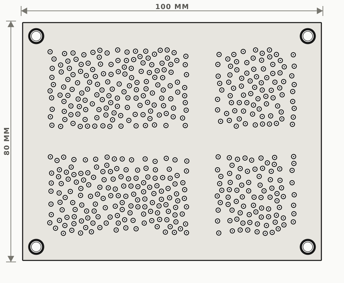
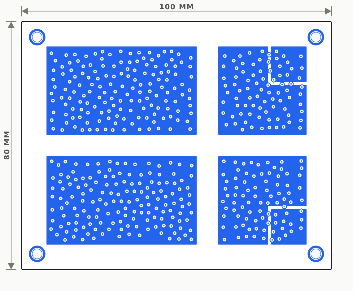
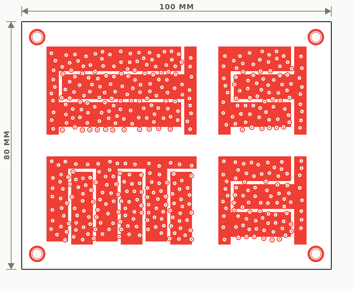
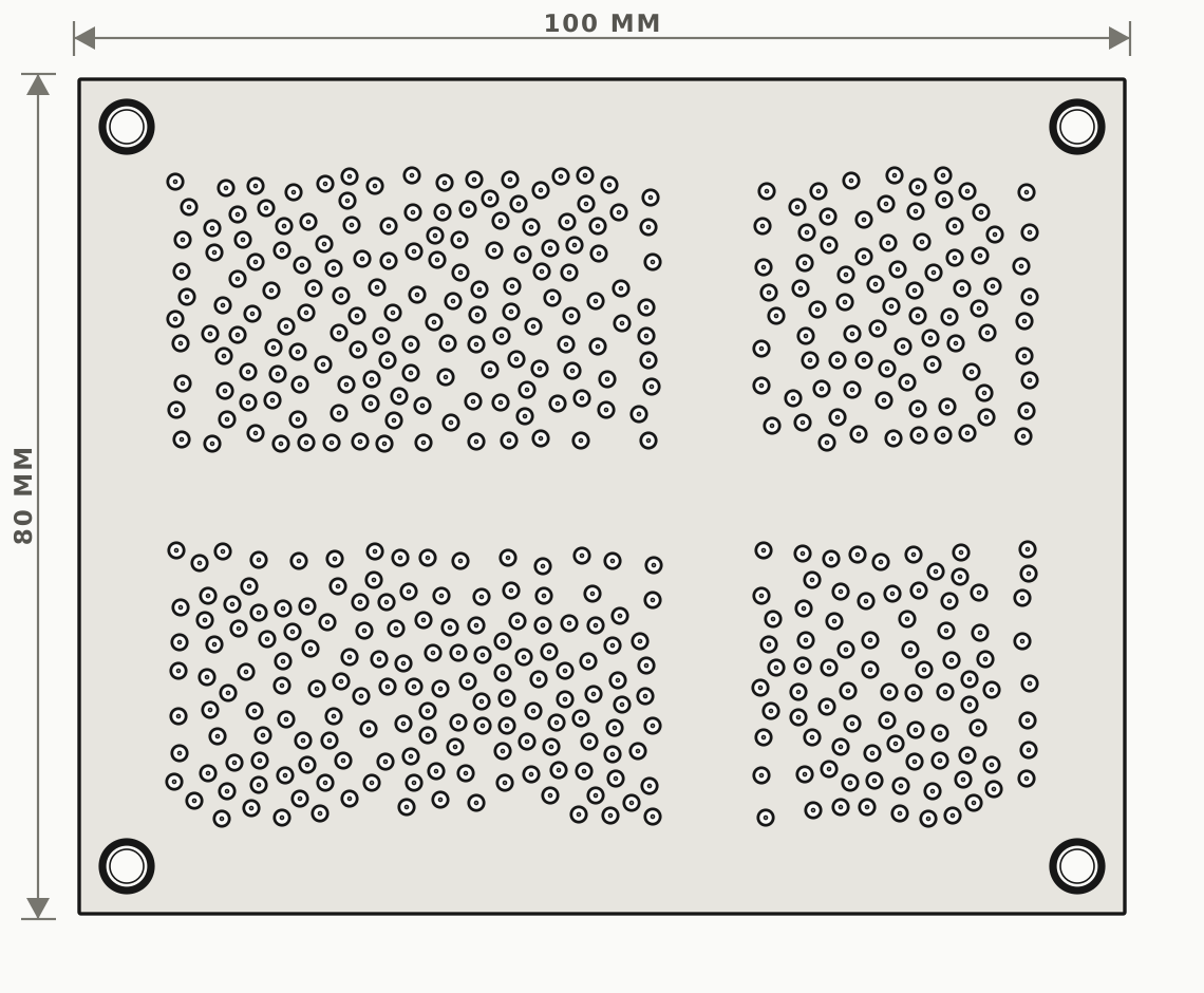
VIA BOARD / PROGRAMMABLE FOUR-LAYER BLANK
One stocked blank. A different four-layer board every time.
The Via Board is manufactured in advance with four copper layers and a dense grid of plated vias. Its outer layers arrive as solid bare copper. A UV laser removes only the copper required by a new design, turning the same ready-to-use blank into that board’s traces, pads, clearances, ground, and power connections.
- L1Solid ablation fieldF.Cu
- L2Six ground islandsGND
- L3Ten power rail islandsPWR
- L4Solid ablation fieldB.Cu
QUESTIONS / STRAIGHT ANSWERS
Know what the system proves and what it does not.
01How autonomous is PromptPCB?+
Give PromptPCB the requirements and it can carry the design from architecture and grounded part selection through schematic, simulation, placement, routing, and release. You can let it run or step in at any point to add constraints, change direction, or approve a decision.
02What does whole-design simulation mean?+
PromptPCB assembles a mixed-model SPICE testbench across the functional design, combining analog, digital, and physics-based models for loads such as motors and batteries. Tests connect each requirement to a measured signal, observed value, acceptance range, and pass or fail result. Anything the available models cannot adequately prove is identified instead of hidden.
03What am I looking at in the waveforms?+
The colored traces are voltages, currents, logic states, or calculated values over time. PromptPCB links each trace to a test and explains the event being checked—for example a load step, a short circuit, startup, braking, or a PWM transition—so the chart is an engineering answer, not decoration.
04Can a passing simulation guarantee the board works?+
No. Simulation covers the models, conditions, and acceptance criteria that were tested. PromptPCB keeps those limits visible. DFM checks, an engineering review, a fabricated first article, and bench validation still matter before volume production.
05What designs are the best fit today?+
PromptPCB is currently strongest on new two-layer robotics, motor-control, and power-conversion boards. Four-layer Via Board designs are supported. BGA, controlled impedance, high-speed interfaces, and RF are beta capabilities and may require additional engineering review.
06Does PromptPCB use real parts?+
Yes. Designs bind symbols, footprints, simulation models, and sourcing records to manufacturer parts from a grounded component library. Missing matches and uncertain data are flagged instead of silently invented.
07What files can I take with me?+
Every release can include the editable schematic and PCB design, purchasable BOM, pick-and-place data, Gerbers, drill files, STEP model, DFM/ERC/DRC evidence, simulation results, waveforms, and test specifications. The outputs use standard formats and can go to JLCPCB or another manufacturer.
08Is the under-two-hour physical board available now?+
Not yet. PromptPCB's software design workflow is available in private preview. The autonomous build cell—UV laser patterning, drilling, pick-and-place, reflow, inspection, physical testing, and immediate revision—is in development, with a target of producing supported prototypes in under two hours.
PRIVATE DESIGN-PARTNER PROGRAM
Bring us a real board.
Help shape the agent.
We are working privately with a small number of robotics and hardware teams. Share a new board requirement or a difficult existing Altium or KiCad design. We’ll evaluate the fit and work with selected partners directly.